
Terms & Conditions
Account Services
My Egchip Account
Sign up for a free Account today. Save ordering information for easy checkout, create and save projects and more.
Update Account Information
Edit your contact, billing, shipping and other account information.
Username/Password Help
Forgot your username or password? Have them emailed to you.
Subscription Center
Sign up for e-mail from chipmarkets or manage your existing subscription preferences.
Ordering Services
Invoices
Search, view, download or print current and past invoices.
My Notes
Associate notes to specific parts and save them when you're logged in to your account.
Order History
Access your current and past orders, view orders with open lines, track shipments and more.
Quote History
Review and order quoted products.
Request Fast Quote (RFQ)
Easily request a single item quote or multiple item quote.
Part Packaging Options
EGchip offers several packaging choices from reels, cut tape and more. Check your parts for these options when ordering.
Newest Products
Learn detailed information and access downloadable resources about Mouser's newest products and latest technologies.
News & Technologies
Learn about the latest applications and industry trends with tutorials and white paper design resources on vertical markets.

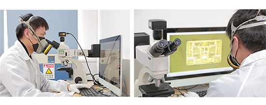
![]() IC Counterfeit Test
IC Counterfeit Test
IC (Integrated Circuit) refers to a chip made by putting many microelectronic components (such as transistors, resistors, capacitors, diodes, etc.) integrated integrated circuits on a plastic substrate. Broadly speaking, the concept of IC chip is a general term for semiconductor component products.
In 2010, due to various factors in the financial market, the domestic IC market and some mainstream IC products have been in short supply since the end of 2009 and the production lines of most manufacturers have stagnated. Due to this phenomenon, a large number of IC terms have appeared in the domestic IC market: bulk new goods, refurbished goods, original goods with original characters, and brand-new original goods.
Bulk new goods: There are two types of bulk new goods. One is the goods that have not been QC and entered the market. The yield is not very high. The other is unused and has no outer packaging. Oxidized goods.
Refurbished goods: This kind of goods passes through some domestic companies that only seek profit margins. The goods returned from various channels are tapped and typed according to model and package, and replaced with a new batch number. And the other is the most terrifying one for purchasers, which is to encapsulate a certain IC with the same model, but not the same brand or IC with the same function. After typing and refurbishing, copy the model. This kind of goods will Purchasing factories has brought great losses.
Original goods: This kind of goods, to put it bluntly, is to disassemble the parts. There are some IC chips that are simple in packaging and can be repeatedly erased. They can be removed by dismantling and exiled to the market for a second time. Goods, the price is generally cheaper.
Brand-new original goods: Needless to say, this kind of goods are all products that the original factory has passed QC certification and entered the market. Generally, the price may be a little higher, but the quality is definitely up to the standard.
IC true and false identification picture:
![]() X-Ray inspection
X-Ray inspection
Description: X-ray test is a real-time non-destructive analysis to check the internal hardware components of the component. It mainly checks the lead frame of the chip, wafer size, gold wire bonding diagram, ESD damage and holes. Customers can provide good products for comparison. examine.
Application scope: detection of internal cracks and foreign body defects in metal materials and parts, plastic materials and parts, electronic components, electronic components, LED components, etc., analysis of internal displacements such as BGA, circuit boards, etc.; distinguishing empty welding and virtual welding Wait for BGA welding defect analysis, etc.
X-Ray inspection picture:

X-Ray inspection equipment picture:
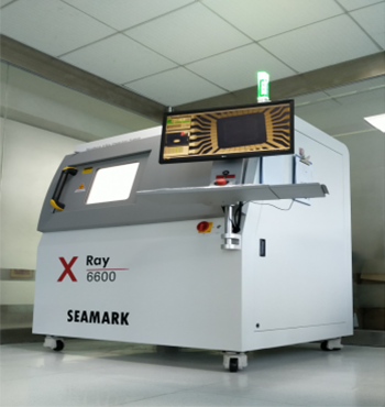
X-Ray inspection introduction:
X-ray (X-ray) detector uses low-energy X-rays without damaging the inspected item to quickly detect the inspected object. The high-voltage impact target is used to generate X-ray penetration to detect the internal structure quality of electronic components, semiconductor packaging products, and the welding quality of various types of solder joints of SMT.
X-Ray inspection content:
1) Defect inspection in IC packaging, such as: layer peeling, burst, void and integrity inspection of bonding;
2) Defects that may occur in the printed circuit board manufacturing process, such as: poor alignment or bridging and open circuit;
3) SMT solder joint void phenomenon detection and measurement;
4) Defect inspection for open circuit, short circuit or abnormal connection that may occur in various connection lines;
5) Integrity inspection of solder balls in solder ball array packaging and chip-on-chip packaging;
6) Inspection of plastic materials with higher density or holes in metal materials;
7) Chip size measurement, wire arc measurement, and component tin area ratio measurement.
X-Ray detection steps:
Confirm the test location and requirements of the sample type/material→Put the sample into the X-Ray fluoroscope inspection table for X-Ray fluoroscopy inspection→Picture judgment analysis→Mark the defect type and location.
X-Ray inspection items:
1. Integrated circuit packaging process inspection: layer peeling, cracking, void and wire bonding process;
2. Printed circuit board manufacturing process inspection: wire offset, bridging, open circuit;
3. Weldability inspection of surface mount technology: inspection and measurement of solder joint voids;
4. Check the connection line: open circuit, short circuit, abnormal or bad connection defect;
5. Integrity inspection of solder balls in solder ball array packaging and chip-on-chip packaging;
6. High-density plastic material cracking or metal material inspection;
7. Chip size measurement, wire arc measurement, and component tin area ratio measurement.
![]() Failure analysis
Failure analysis
Description: Through professional failure analysis equipment, using various test analysis techniques and analysis procedures to confirm the failure phenomenon of electronic components, distinguish its failure mode and failure mechanism, confirm the final failure cause, and put forward suggestions for improving the design and manufacturing process to prevent Recurring failures.
Application Scope: Analysis of the causes of all failed devices.
Application failure analysis picture:

Basic concepts of failure analysis
1. Failure analysis often requires electrical measurement and the use of advanced physical, metallurgical and chemical analysis methods.
2. The purpose of failure analysis is to determine the failure mode and failure mechanism, and propose corrective measures to prevent the recurrence of this failure mode and failure mechanism.
3. Failure mode refers to the observed failure phenomenon and failure form, such as open circuit, short circuit, parameter drift, functional failure, etc.
4. Failure mechanism refers to the physical and chemical process of failure, such as fatigue, corrosion and overstress.
The significance of failure analysis
1. Failure analysis is a necessary means to determine the failure mechanism of a chip.
2. Failure analysis provides necessary information for effective fault diagnosis.
3. Failure analysis provides necessary feedback information for design engineers to continuously improve or repair the chip design to make it more consistent with the design specifications.
4. Failure analysis can evaluate the effectiveness of different test vectors, provide necessary supplements for production testing, and provide the necessary information basis for verifying the optimization of the test process.
The main steps and content of failure analysis
Unpacking the chip:
Remove the IC encapsulant while keeping the chip function intact, keeping die, bondpads, bondwires and even lead-frame from damage, preparing for the next step of chip failure analysis experiment.
SEM scanning electron microscope/EDX component analysis:
Including material structure analysis/defect observation, element composition routine micro-area analysis, accurate measurement of component size, etc. Probe test: Use micro probes to quickly and easily obtain the internal electrical signals of the IC.
Laser cutting:
Cut a specific area on the circuit or chip with a micro laser beam.
EMMI detection:
The EMMI low-light microscope is a highly efficient failure analysis tool that provides a highly sensitive and non-destructive fault location method that can detect and locate very weak light (visible light and near-infrared light), thereby capturing various Visible light for leakage current caused by component defects or abnormalities.
OBIRCH application (laser beam induced impedance change test):
OBIRCH is often used for high-impedance and low-impedance analysis inside the chip, and line leakage path analysis. Using the OBIRCH method, it is possible to effectively locate defects in the circuit, such as holes in lines and holes under through holes. The high-resistance area at the bottom of the through hole can also effectively detect short circuits or leakage, which is a powerful supplement to the luminescence microscopy technology.
LG LCD hot spot detection:
Using the liquid crystal sensor to detect the molecular arrangement and reorganization of the IC leakage, it shows a patchy image different from other areas under the microscope. Find the leakage area that troubles the designer in the actual analysis (the fault point of more than 10mA).
Fixed-point/non-fixed-point chip grinding:
Remove the gold bumps implanted on the LCD driver chip Pad to keep the Pad intact for subsequent analysis or rebonding.
X-Ray non-destructive detection:
Detect various defects in IC packaging such as layer peeling, bursting, voids, and integrity of wire bonding, possible defects in the PCB manufacturing process such as poor alignment or bridging, open circuit, short circuit or abnormal connection defects, and solder balls in the package Completeness.
SAM (SAT) ultrasonic flaw detection:
Non-destructive inspection of the internal structure of the IC package can effectively detect various damages caused by moisture or heat, such as: o wafer surface delamination, o solder balls, wafers or cracks in the filler, o packaging The pores in the material, o various pores such as the pores in the wafer joint surface, solder ball, filler, etc.